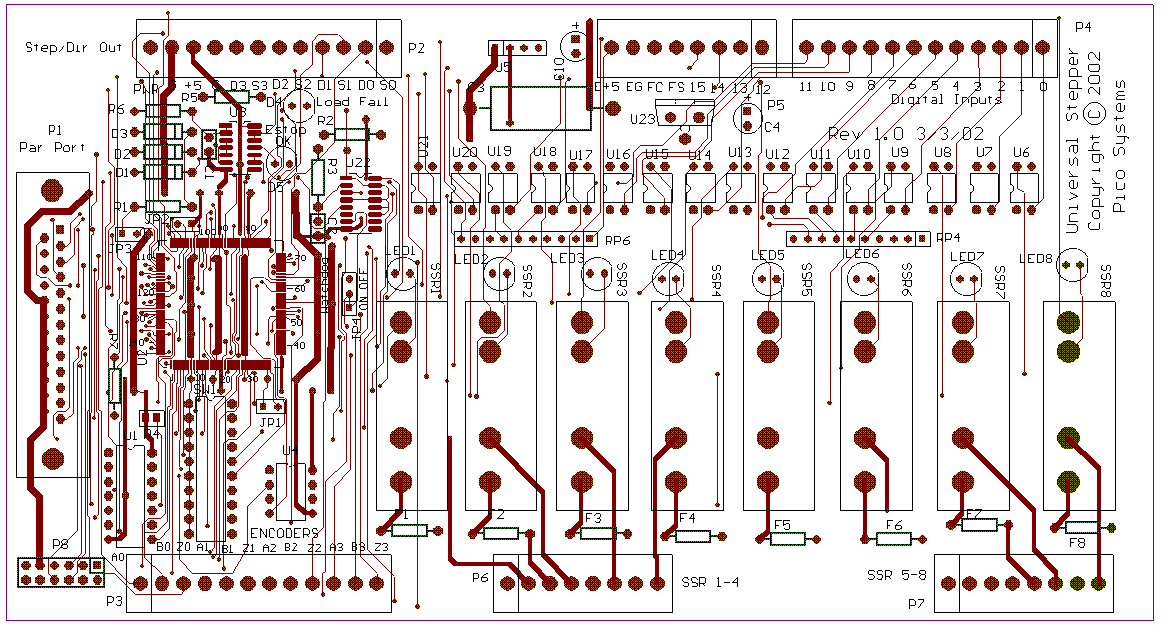
 Board Layout
| P1 connects to the PC parallel port. |
| P3 Pin # | J3 Pin # | Board Marking | Signal |
| 1 | 1 | A0 | Axis 0 A |
| 2 | 2 | B0 | Axis 0 B |
| 3 | 3 | Z0 | Axis 0 Z (index) |
| 4 | 4 | A1 | Axis 1 A |
| 5 | 5 | B1 | Axis 1 B |
| 6 | 6 | Z1 | Axis 1 Z (index) |
| 7 | 7 | A2 | Axis 2 A |
| 8 | 8 | B2 | Axis 2 B |
| 9 | 9 | Z2 | Axis 2 Z (index) |
| 10 | 10 | A3 | Axis 3 A |
| 11 | 11 | B3 | Axis 3 B |
| 12 | 12 | Z3 | Axis 3 Z (index) |
| 13 | Ground | ||
| 14 | + 5 V Power |
| A and B are the quadrature signals from the encoder. If you have an encoder with an index channel, this is connected to the Z input. If no encoder, connect S0 to Z0, S1 to Z1, etc. If you have an encoder without the index channel, connect A to Z for each axis. |
| P2 connects to the stepper drivers, and also provides unregulated power to the board, and regulated +5 V can be taken from the board to supply encoders. J2 does not provide the unregulated power to the board, otherwise all the other signals are available. Pins are as follows : |
| P2 Pin # | J2 Pin # | Board Marking | Signal |
| 1 | 1 | S0 | Step to Axis 0 |
| 2 | 2 | D0 | Direction to Axis 0 |
| 3 | 3 | S1 | Step to Axis 1 |
| 4 | 4 | D1 | Direction to Axis 1 |
| 5 | 5 | S2 | Step to Axis 2 |
| 6 | 6 | D2 | Direction to Axis 2 |
| 7 | 7 | S3 | Step to Axis 3 |
| 8 | 8 | D3 | Direction to Axis 3 |
| 9 | 13 | G | power ground (same as P2-11) |
| 10 | 14 | +5 | +5 Volt output |
| 11 | G | power ground | |
| 12 | PWR | Unregulated power in |
| P4 and P5 connect to the digital input contact closures, and also provide isolated +5 V power for these switches. J4 brings out the same connections in ribbon cable header form. P5-7 and P5-8 are a source of isolated 5 V power from an on-board DC-DC converter, to be used for the digital inputs. For each input, a switch is connected between that input and P5-7. P4 Pins are as follows : |
| P4 Pin # | J4 Pin # | Board Marking | Signal | Function |
| 1 | 1 | 0 | Bit 0 input | X Home |
| 2 | 2 | 1 | Bit 1 input | -X Limit |
| 3 | 3 | 2 | Bit 2 input | +X Limit |
| 4 | 4 | 3 | Bit 3 input | available |
| 5 | 5 | 4 | Bit 4 input | Y Home |
| 6 | 6 | 5 | Bit 5 input | -Y Limit |
| 7 | 7 | 6 | Bit 6 input | +Y Limit |
| 8 | 8 | 7 | Bit 7 input | available |
| 9 | 9 | 8 | Bit 8 input | Z Home |
| 10 | 10 | 9 | Bit 9 input | -Z Limit |
| 11 | 11 | 10 | Bit 10 input | +Z Limit |
| 12 | 12 | 11 | Bit 11 input | available |
| P5 Pin # | J4 Pin # | Board Marking | Signal | Function |
| 1 | 13 | 12 | Bit 12 input | available |
| 2 | 14 | 13 | Bit 13 input | available |
| 3 | 15 | 14 | Bit 14 input | available |
| 4 | 16 | 15 | Bit 15 input | closed for E-Stop OK |
| 5 | 17 | FS | (Not Used) | |
| 6 | 18 | FC | (Not Used) | |
| 7 | 19 | EG | Isolated Ground | other end of switches |
| 8 | 20 | E+5 | Isolated +5 Source |
| P6 and P7 bring out the Solid State Relay terminals. Each output is separately fused, and isolated. P6 Pins are as follows : |
| Pin # | Signal |
| 1 | SSR 1 source |
| 2 | SSR 1 load |
| 3 | SSR 2 source |
| 4 | SSR 2 load |
| 5 | SSR 3 source |
| 6 | SSR 3 load |
| 7 | SSR 4 source |
| 8 | SSR 4 load |
| Pin # | Signal |
| 1 | SSR 5 source |
| 2 | SSR 5 load |
| 3 | SSR 6 source |
| 4 | SSR 6 load |
| 5 | SSR 7 source |
| 6 | SSR 7 load |
| 7 | SSR 8 source |
| 8 | SSR 8 load |
| Pin # | Signal |
| 1..8 | Least significant bit .. Most significant bit |
| 9 | Ground |
| 10 | + 5 V |
| 11 | Not-Reverse |
| 12 | Not-Forward |
| Board Layout |