|
Well, I wanted to move up from 8-bit systems,
so I started building a 32-bit bit-slice system
using AMD 2903 ALU chips and the 2910 sequencer.
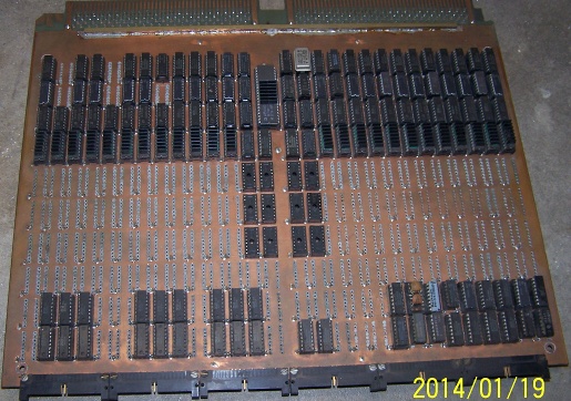
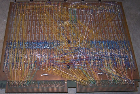
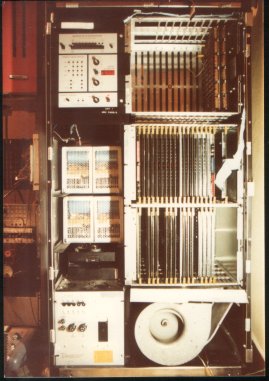
I built one board with the sequencer and 1 K (expandable to 4K)
words of 96 bits for control storage, and the ALU board with
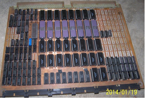
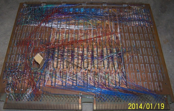
56 32-bit registers and the 2903s and fast carry
chips. This all had a bunch of diag/control
hardware that ran off the CP/M system, so you
could force single instructions into the
instruction register and single-cycle execute them,
read the data bus, load a program into the
control store, etc. I wrote a very sophisticated
interface program for controlling and debugging
the bit-slice system. You could load a program,
start and stop execution, examine and alter
registers and so on.
I started writing microcode,
using a micro-assembler built in the CP/M
macro assembler, and found it to be VERY tedious.
I could write a only few instructions per evening!
I did write multiply and divide routines and
test those, as well as a few other things.
I obtained a cast-off 1 MB memory off the
university's 370/145. (A friend of mine
got the two 370/145 CPUs and the other memory
box. Trying to power the 370 up on a 60 A 240 V
service was a fool's errand. We were lucky to
not blow the transformer off the pole!)
Anyway, I still had to build a general bus for the
system, and then interface the memory to the
bus before I could do much of anything. Then,
I'd have to complete the microcode, and come up
with an OS for the system. And, I'd left for later
putting in the hardware to make N-way branches from
the op-code, and or in the register select fields
to select registers from the register stack. Not that
difficult, but it would mean ripping up a lot of wire-wrap
that was already tested.
My plan was to follow
the general scheme of the IBM 360, but add
stack instructions. But, it would end up not being
much like a 360 architecture, as I was planning
to use memory-mapped controllers much like a
PDP-11, instead of IBM-style channels. So, I'd
be on my own for an OS, at least. (Well, I sure
wouldn't want to be running OS/MFT and JCL on it.
GAACK!) This was all starting to sound
like a really daunting project, but I was still
fiddling with it.
|